

RTP – Rapid Thermal Processing
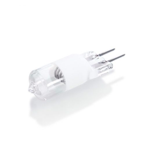
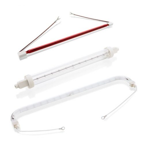
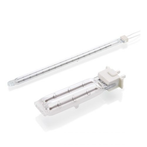
Ushio’s infrared (IR) lamp solutions have a long history of implementation in the production of semiconductor wafers. Rapid thermal processing (RTP) is a fast, contact-free IR heat irradiation process which prevents wafer contamination. Ushio delivers infrared Rapid Thermal Procession lamps, with heating power of several kilowatts, in the form of specially designed single and double-ended infrared emitters.
Ushio’s latest brochures and product catalogues can be found on our downloads page. If you are ready to make a formal enquiry, please fill in the form on our contact page.
What is Rapid Thermal Processing (RTP)?
Rapid Thermal Processing (RTP) is a heating and cooling procedure predominantly associated with semiconductor manufacturing and solar cell fabrication. RTP involves heating silicon wafers to an extremely high temperature, often well over 1000°C, by means of a high-intensity infrared emitting lamp. After a short period of heating, the wafer sample is then slowly cooled. This method of processing, sometimes referred to as Rapid Thermal Annealing (RTA), is designed to adjust the electrical properties of the semiconductor material.
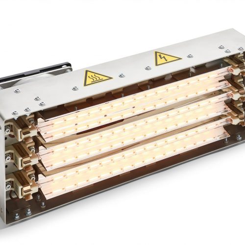
Our lamps can be installed as the central rapid heating component of your RTP furnace and linked to the built-in pyrometer and thermocouples which regulate your output temperature. The period of ramped heat may last milliseconds, or as much as 60 seconds, before the temperature is carefully reduced at a rate which minimises thermal shock. Thermal shock can cause dislocations, imperfections, and/or catastrophic destruction of the wafer sample.
Ushio has many years of experience in the delivery of specially designed single and double-ended IR emitters. Guaranteeing heating power of several kilowatts, your Ushio lamp can be customised to integrate into any industrial RTP scenario.
Desired Effects and Capabilities of Rapid Thermal Processing (RTP)
- Dopant activation – the alteration of the electrical properties of a substrate by a heating process, following the ion implantation of dopants, is referred to as dopant activation. The ions of dopants such as phosphorus, arsenic, and boron are stimulated by thermal energy which alters the electrical characteristics of the entire substrate. A crucial factor in this process is the ability to accurately and quickly control temperature and ramp rates due to the time and temperature sensitivity factors involved. A modern RTP system should be able to control diffusion by regulating the extreme temperatures to within one degree Celsius.
- Surface defect passivation – the enhancement of power conversion efficiencies (PCE) and substantial stability improvement in the surface of polycrystalline (perovskite) solar cells. The semiconductor surface becomes inert, but the conduction properties are unaffected and nullify any surface states which may affect the passage of electricity through the cell – most notably, extreme weather conditions. This method, sometimes referred to as the Atalla passivation technique, is a method of thermal oxidation.
- High-temperature wet oxidation / Rapid Thermal Oxidation (RTO) – the high temperature diffusion of an oxidising agent, such as silicon oxide, into the semiconductor wafer sample. This process gave rise to the complimentary metal-oxide semiconductor (CMOS).
- Densification of deposited films – densification and crystallisation is carried out to achieve total elimination of any residual porosity or structural free volume in the deposited film. This often takes place with the removal of any residual solvents or other organics present on the surface in a combined process.
- Lattice damage repair – during ion implantation doping, damage to the semiconductor crystal lattice occurs and the implanted ions are not yet electrically active. RTP applies a thermal anneal which repairs the damage and enables the implanted dopants.
- Metal / Solder Reflow – a process which allows the soldering of surface-mount devices (SMD) directly onto a printed circuit board (PCB). The vital requirement in metal reflow is the precise control of temperature, where full liquidity must be achieved on all solder joints without overheating any of the surface mounted components or materials. If the temperature of the reflow is uneven, the solder will complete its wetting and setting processes at different times. In a side-effect known as PCB “tombstoning”, one end of an SMD partially lifts away from the PCB causing an open circuit and rendering the entire design useless.
- Rapid Thermal Chemical Vapour Deposition (RTCVD) – A modern form of surface modification, CVD is used to augment the surface of a substrate through the deposition of thin layers of material. The rapid heating method heats only the wafer substrate, rather than the ambient gas or furnace walls, which serves to minimise undesirable particle formation within the treated material. A variety of films are used in this process, such as gallium arsenide (GaAs) in the production of photovoltaic devices.
- Contact alloying – During the creation of a metal-semiconductor interface, a high temperature annealing stage is required to alloy the deposited metal contacts with the semiconductor material. Adding further dopants to the process can improve the Ohmic contact, and forming a highly doped region at the point of interface.
- Silicide and barrier layer formation – a layer of oxide exists on the top layer of the semiconductor material. A substance can be added to this layer to increase the adhesive qualities of the photoresist coating to be applied in the next phase; however the ensuing chemical reaction catalyses further oxidisation to form a hydrophobic barrier layer. This layer prevents the developing agent from entering the region between the photoresist and the wafer and “lifting” essential formations from the semiconductor surface.
For more information about Ushio’s Rapid Thermal Processing (RTP) lamp solutions for PCB and semiconductor production, please visit our contact page.