
UV Lithography for Semiconductor and PCB Fabrication
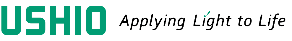
Ushio offers a complete range of ultraviolet (UV) lithography solutions suitable for all major photolithography equipment manufacturers. Our business supplies highly reliable lamp solutions to optimise the cost of ownership in the semiconductor integrated circuit (IC) production process: long-life products combined with high intensity technologies guarantee a cost-efficient and high throughput production process.
Jointly developed with device manufacturers in response to their increasingly diverse needs, Ushio’s lithographic UV lamps have earned high acclaim as well as user trust. From our broad range of lamps, we can offer optimal irradiation solutions to bolster your productivity and improve yields. We can also supply component lamps tailored for integration into new lithography devices developed by your own in-house experts.
Ushio’s lighting solutions are widely used during the cleaning and exposure phase of the process, in which manufacturers project IC patterns onto a substrate by focusing ultraviolet wavelength radiation through a photomask, onto a photosensitive chemical layer called a photoresist.
What is Lithography?
The term lithography, which derives from the Greek words litho- (stone) and graphein (to draw), was originally used to describe an impression printing technique which involved etching designs into stone. Once the stone cut design was completed, ink could be used to mass produce prints of the design across various media.
In the case of semiconductor, UV lithography or photolithography is the microfabrication process used to optically form geometric patterns on to a semiconductor wafer for the mass production of integrated circuits (IC) and computer chips.
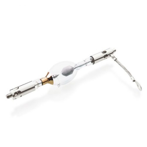
Wafer Cleaning
The presence of contaminants on the surface of semiconductor wafers can lead to cause them to be driven into the material during production, which can lead to an inferior product that has a diminished ability to perform as a good semiconductor.
For this reason, the wafers must be prepared in a cleanroom scenario and undergo stringent wafer cleaning procedures before proceeding with the rest of the lithography process. While much of this cleaning involves solvent chemicals, Ushio provides light-based alternative solutions which can be explored in more detail by visiting our dedicated Semiconductor Wafer Cleaning page.
Barrier Film Formation
A layer of oxide exists on the top layer of the semiconductor material. A substance can added to this layer to increase the adhesive qualities of the photoresist coating to be applied in the next phase; however the ensuing chemical reaction catalyses further oxidisation to form a hydrophobic barrier layer.
This layer prevents the developing agent from entering the region between the photoresist and the wafer and “lifting” essential formations from the semiconductor surface.
Photoresist Coating
A photoresist coating, also known simply as a resist, is a UV-sensitive material which is deposited onto the semiconductor wafer surface. There are two types coating used: positive photoresist and negative photoresist. Usually the photoresist is applied using a spin coating method.
When exposed to UV radiation, a positive photoresist becomes soluble and can be removed during the developing phase. Any part of the photoresist coating which is not exposed to UV radiation will remain on the surface.
In the case of negative photoresist coatings the reverse takes place, in which the UV exposed coating becomes insoluble. Any part of the photoresist coating which is exposed to UV radiation will remain on the surface, and the photoresist which remains unexposed will be removed during the developing phase.
The most commonly used type is the positive photoresist coating. The photoresist coating performs the vital function of resisting the etchants, which will be applied during the etching phase later on.
Photomasking / UV Exposure
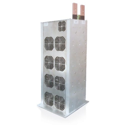
This phase in the lithography process is where Ushio’s proven mastery of UV technology really excels itself. Our high wattage mercury short arc lamps are calibrated to emit UV radiation at the desired wavelength for your specific photolithography process, thereby maximising treatment speed and providing a cost effective UV exposure solution.
The layered patterns to be constructed upon the semiconductor surface are created, almost like blueprints, on a series of photomasks. The photomask is positioned over the photoresist coated wafer before UV radiation is directed towards it. The areas of photoresist which are masked do not receive any exposure to the UV waves; however the unmasked areas receive full exposure.
The resulting chemical change means some of the photoresist is susceptible to removal by a developing solution. Whether it is the exposed or unexposed coating which will be removed depends on which type of photoresist is used, positive or negative. For the purposes of clear understanding, we will assume that a positive photoresist has been used prior to the developing stage.
Developing
A chemical developing solution is added to the surface of the photoresist, in order to dissolve areas of positive photoresist which were unmasked during exposure. At this stage, a baking process must take place in order to strengthen the protective qualities of the remaining photoresist in preparation for the etching phase.
Etching
The etching process seeks to remove the oxidised barrier layer, located between the semiconductor surface and the photoresist layer, which is uncovered as a result of the exposure and developing stages. The remaining photoresist-coated oxidised regions are protected from the etchant, creating a patterned cavity which reaches the all the way down to surface of the semiconductor.
Photoresist Removal
After the etching phase is completed, the photoresist is no longer required and must be removed from the substrate. This can be achieved in a number of ways, including chemical stripping or plasma ashing.
Contact Ushio for top quality UV lithography advice and solutions
With vast expertise at our disposal, Ushio is ready to advise your team on how to implement our UV components into your lithography system solution. To receive top class advice from our dedicated semiconductor team, please begin your enquiry by filling in the form on our contact page. Additionally, Ushio’s latest brochures and product catalogues can be found on our downloads page.