Ushio Inc. is proud to announce the development of a new high-power LED package called the “EDCC Family,” designed with a focus on compactness and high-density integration. Production of the EDCC Family is set to commence in the first quarter of 2024.
The EDCC Family incorporates traditional high-power LED chips with a wide range of wavelength options, yet it achieves an impressive reduction in footprint of approximately 80% when compared to the previous small-sized EDC Family package. As a result, it offers a compact form factor (W1.5 x L1.85 x H0.9 mm) that closely resembles bare chips and is also compatible with CSP (Chip Scale Package) and other compact-sized packages. This ensures not only ease of customization but also the convenience of handling SMD (Surface Mount Device) packages.


Key Features
・Utilizes high-power LED chips with a wide wavelength range, including UV, visible light, IR, and SWIR, similar to those used in the SMBB Family and EDC Family.
・Compact-sized package, comparable to CSP and high-power LED chips, facilitating easy customization in an SMD-type LED format.
・Package design optimized for high-density integration.
Applications
The EDCC Family is suitable for a wide range of applications that require high brightness, high output, and the combination of multiple wavelengths, including but not limited to:
・Machine Vision
・Optical Sorting
・Plant Growth
・Security
・Surveillance Cameras
・Optical Authentication
・Inspection Equipment
・Vital Sensing and more.
Comparison with conventional products
| SMBB Flat | EDC Flat | EDCC | |
| Package area(mm) | 5.0×5.2 | 3.5×3.5 | 1.5×1.85 80% reduction compared to EDC Family |
| Appearance |  |  |  |
Comparison
| SMBB850DS-1100 | EDC850DS-1100 | EDCC850DS-1100 | ||
| Vf[V]@1A | 3.2 | 3.2 | 3.2 | |
| Vfp[V]@5A* | 4.6 | 4.6 | 4.6 | |
| Po[W]@1A | 1.4 | 1.4 | 1.2 | |
| Po[W]@5A* | 5.6 | 5.6 | 5.3 | |
| Rthjs[K/W] | 9 | 11 | 21 | |
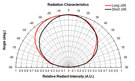
| φ1/2[deg.] | 64 | 66 | Long** | 69 |
| Short** | 66 | |||
*Pulse Condition: On Time 10us, Duty 1%
**Radiation Characteristics of EDCC Package


Package Design Optimized for High-Density Integration
The EDCC Family features a package design specifically tailored for high-density integration.
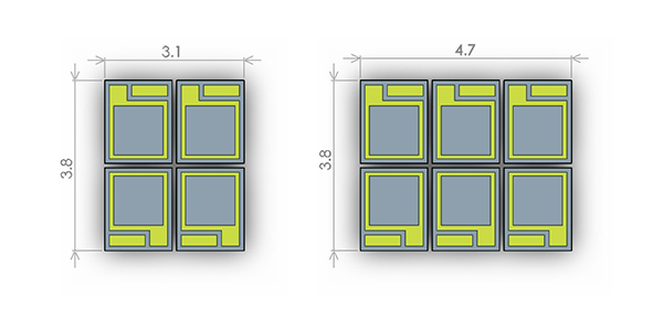
When EDCC packages are arranged in a 2 x 2 configuration, they fit within a compact 4mm x 3.2mm footprint, offering a package size nearly equivalent to the EDC package. Even when arranged in a 2 x 3 configuration, the total footprint remains compact at 4mm x 4.9mm, surpassing the SMBB package in terms of package area efficiency.
<Example of LED placement>

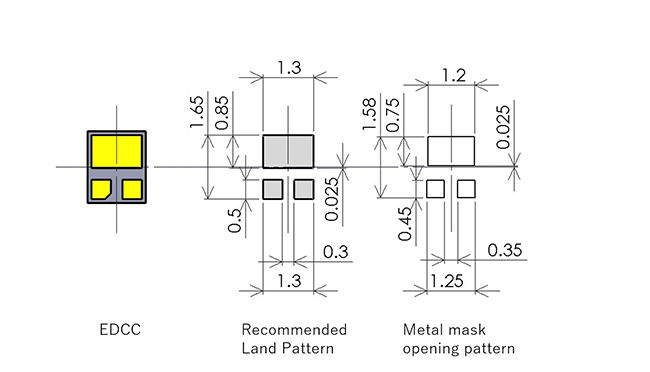
<Recommended Land Pattern/Metal Mask Aperture Pattern>

Release Date
| Range | Release Date | |
| UV | 365nm-420nm | TBD |
| Visible | 430nm-680nm | 2024 1Q |
| NIR | 690nm-980nm | 2024 1Q |
| SWIR | 1050nm-1900nm | 2024 1Q |
Engineering Sample List
Single Junction Type
| 670nm: EDCC670D-1100-X | 780nm: EDCC780D-1100-X | 940nm: EDCC940D-1100-X | 1150nm: EDCC1150D-1100-X | 1550nm: EDCC1550D-1100-X |
| 700nm: EDCC700D-1100-X | 810nm: EDCC810D-1100-X | 970nm: EDCC970D-1100-X | 1200nm: EDCC1200D-1100-X | 1650nm: EDCC1650D-1100-X |
| 720nm: EDCC720D-1100-X | 850nm: EDCC850D-1100-X | 1050nm: EDCC1050GD-1100-X | 1300nm: EDCC1300D-1100-X | 1900nm: EDCC1900D-1100-X |
| 740nm: EDCC740D-1100-X | 890nm: EDCC890D-1100-X | 1070nm: EDCC1070D-1100-X | 1370nm: EDCC1370D-1100-X | |
| 760nm: EDCC760D-1100-X | 910nm: EDCC910D-1100-X | 1100nm: EDCC1100D-1100-X | 1450nm: EDCC1450D-1100-X |
Dual Junction Series
| 810nm: EDCC810DS-1100-X | 890nm: EDCC890DS-1100-X | 970nm: EDCC970DS-1100-X |
| 850nm: EDCC850DS-1100-X | 940nm: EDCC940DS-1100-X |
* Models with “-X” in their part numbers are exclusive to prototypes and engineering samples, and the part numbers will change for mass production.
* Please note that this product is under development and may be subject to changes and modifications without prior notice.
Product and Engineering Sample Inquiries
We have a limited quantity of engineering samples available for the EDCC package.
For inquiries, please click here.
More Information
For more product information, please click here.


